 |
Electronics Tutorial The purpose of this tutorial is to explain my electronics plans for persons who have an interest in electronics but do not understand all of the details. Therefore, it is organized to explain the plans. What I think anyone is supposed to see in the amplifier design is that it brings amplifiers up to the level of the rest of modern electronics. It replaces a bunch of finicky and expensive witchcraft with reliable, predictable, cheap and effective electronics. The current amplifier needs to be put on power integrated circuits, but that isn't happening, because the electronics industry doesn't want a nonprofessional telling them how to do things, particularly when they see money to be made in expensive and corrupt products. The Femto Capacitance Meter needs to be viewed in the following perspective: I once bought some high quality fractional picofarad NPO capacitors in a grab-bag sale. Each capacitor of a size was the same but off by 20-40%. It means the manufacture could produce highly precise capacitors but couldn't measure what was being manufactured. The FCM cannot be battery power when using home-builder techniques, because it needs too much current and voltage. But there is no reason for it to be battery powered, because capacitors cannot be measured in-circuit, and there is an advantage to leaving the device on without running down batteries.
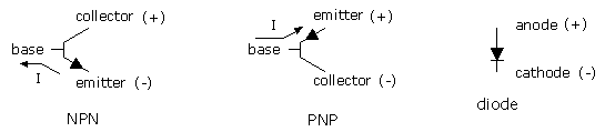
The current is shown to flow in the actual direction which the electrons move. The electricians have a practice of showing "conventional current" as flowing in the opposite direction, because someone had it backwards in the nineteenth century. I show actual current direction instead of conventional current direction. The arrow inside the transistor shows the base-emitter junction. It is the same as a diode. It always has approximately 0.6V across it while current is flowing through it. But the deviations are important. So here's the story on that. Higher beta (current gain) results in more voltage at that junction. The small signal transistors with betas of 300 or more will have 0.65V or more on that junction. Power transistors might have 0.57V. As more current is drawn through the bases, the voltage increases, sometimes to 1V or more. It decreases upon heat-up, perhaps to 0.4V at 100°C. Diodes make good temperature sensors, because the voltage change with temperature at that junction is linear, while thermistors are not linear; and diodes are about half as sensitive as thermistors, which is acceptable. On top of that, diodes are smaller in mass than thermistors, which reduces heat capacity and response time. The beta (or hFE) of a transistor is current gain defined as the current through the collector divided by the current through the base. For convenience, it's easier to measure the current through the emitter instead of the collector. The error is the inverse of the beta, which isn't much. Some meters have beta testers on them, which is a good feature to look for. The base-collector junction is almost identical to the base-emitter junction. If you test it with a diode tester, you will notice that it is slightly lower voltage due to larger surface area. The voltage gain of a transistor is determined by circuit resistance. It is approximately the resistance at the collector divided by the resistance at the emitter. This means resistance to any hard voltage, which sometimes would be a supply rail. Sometimes a capacitor paralleling a resistor is used for hard ac voltage. For example, if there is a 10K resistor at the collector, and a 1K resistor at the emitter, the voltage gain is 10. This means a 1V change on the base will show a 10V change at the collector, but it will be inverted. Inverted means that while the base increases in voltage, the collector decreases in voltage. While collectors are used for voltage gain, emitters are used for current gain. The current gain is approximately the same as the beta. While there is no voltage gain at the emitter, there is an offset voltage equal to the base-emitter voltage of approximately 0.6V. Operational Amplifiers
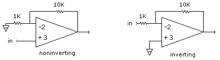
Noninverting amplifier means the output voltage increases when the input voltage increases. But there is usually a voltage gain. The gain formula for a noninverting amplifier is feedback resistance plus input resistance divided by input resistance. In the example, it is 10K + 1K ÷ 1K = 11. Inverting amplifier means the output voltage decreases when the input voltage increases. The gain formula is feedback resistance divided by input resistance. In the example, it is 10K ÷ 1K = 10. An important difference is the input impedance or current. The noninverting amplifier has very high input impedance, and consequently very low input current, because the signal goes directly to the input. But for the inverting amplifier the input impedance is the input resistor. When there is 1V input through the 1K resistor, the input current is 1mA. An important thing to notice about op amps is that the two inputs always function at the same voltage except for offset voltage, which is typically a few mV. Often, the offset voltage is removed, either through offset adjustment pins, or through an adjustment circuit. This means that when the +3 pin is grounded on the inverting amplifier, the -2 pin functions at ground voltage plus offset voltage. There is another source of slight difference in input voltages. The functional, differential voltage on the input pins will be the output voltage divided by the internal gain, which is typically 50,000.
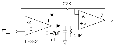
A peak detector determines the peak voltage on an ac wave and converts it into a dc voltage. A diode puts the peak voltage on a capacitor. The second op amp is a buffer. This means it holds the same voltage input and output, but it allows current to be used at the output without altering the voltage. An op amp buffer is created by connecting the output to the inverting input. The purpose of the buffer in this instance is to tell the first op amp what the voltage is on the capacitor. In simple designs, this is done by simply connecting the inverting input of the first op amp directly to the capacitor. But the buffer allows a second diode to be used in the feedback loop without altering the capacitor voltage. The diode then pulls against the output of the buffer instead of the capacitor. The purpose of the feedback diode is to prevent the output from saturating on the down-swing. Saturation means the output goes to the supply rail, while excess current is drawn through the input, which can create undesirable effects. The feedback diode pulls the inverting input down to the same level as the noninverting input, which means the output is never more than 0.6V lower than the noninverting input or the bottom of the voltage swing on the ac input wave. The feedback resistor allows a difference in voltage to be created between the inverting input and the output of the buffer. The design challenge of a peak detector is in the fact that the diode pulls the voltage up but not down. Something needs to bring the dc voltage on the capacitor back down, either when the voltage being measured decreases, or when an over-voltage spike is created for some reason such as noise, contact of leads or turn on of the device. Leakage current through the diode when reverse biased will be enough to control the capacitor voltage when stable measurements are being made. At other times, more current is needed to bring the capacitor voltage down. A resistor can be used for that purpose. But it will then create some ripple on the capacitor, because it will be pulling voltage down while the diode is not pulling it up. The ripple is greatest for lowest frequencies, because then there is more time during each cycle for voltage to decrease. Therefore, low frequencies require some compromise between ripple on the dc and rate of equilibration. Here's how to calculate ripple on the capacitor. Start with this formula: V/S = I/C. It says volts per second equals current over capacitance. Say there is one volt on the cap. Divided by 10M of resistance equals 0.1µA of current. Divided by 0.47µF equals 0.213 volts per second. If the frequency is 10Hz, there is 0.05 seconds for each half of the wave. So 0.213V/S times 0.05S equals 11mV of ripple. If the frequency is increased to 1KHz, a half wave is 0.5mS, and ripple is 0.0005 × 0.213 = 0.11mV. If the cap voltage is increased to 2V, the ripple is 0.21mV, or twice as much, but the same percent. The rate at which the voltage equilibrates is not linear. At 1V on the cap, it is 0.213 volts per second; but at 2V, it is 0.426V/S. So it would take about 3-5 seconds to equilibrate when 1V too high. Pulling it down instantly with a push button switch is so easy that it is better than compromising the design or waiting for equilibration. Additional Info.
By Gary Novak |
|
|
||||||||||||