 |
The First Precision Meter for Small Capacitors
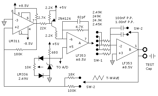
Introduction The Femto Capacitance Meter measures in the low femtofarad area having a resolution of 10 femtofarads (fF). The meter has six ranges allowing a maximum measurement of 4 microfarads. This allows one picofarad to be measured with 1% error. The need for this is in the fact that the best meters by previous designs would have 20-50% error on 1pF. This precision requires elimination of test leads. Instead insertion pins are used. Since capacitors are not measured in-circuit, there are advantages in removing test leads which create clutter. The theory starts with the formula for analyzing capacitance. It is this:
It says: capacitance equals current over volts per second. It means that if one side of a capacitor is grounded and a constant current is applied to the other side, the voltage will increase at a constant rate. Measuring the rate of voltage increase is the usual method of determining the capacitance. But it doesn't work well for small capacitors, because timing between two reference voltages in a small amount of time is difficult. However, the procedure is quite precise at low speeds; and it can be used for measuring reference capacitors, as shown later. What the femto capacitance meter does is hold the volts per second constant while measuring the current. Current can be measured at high speeds easier than volts per second can. One of the advantages is that the circuits are totally analog; so the resolution is limited only by noise. The circuits are fortuitously highly immune to noise, because three capacitors function as noise filters - a reference capacitor, the capacitor being measured and a peak detector capacitor. The constant volts per second are produced by a precision triangle wave generator. Applying the triangle wave to one side of the capacitor being measured results in a constant current on the other side. The current is detected with a current-to-voltage converter which has a square wave at the output. A peak detector measures the amplitude of the square wave. The resulting voltage is put on a digital display through an analog-to-digital converter, which is a voltmeter on a chip. A digital voltmeter could be used for reading. (Gaining voltage by 2 may be needed, as explained under Current-to-voltage Converters.)
Triangle Wave Generator The triangle wave generator uses the standard procedure, except that a reference voltage is added for high precision. Let's look at the details starting with the comparator (LM311). It produces the change of state when the amplitude of the triangle wave reaches the appropriate points. The amplitude of the T-wave is not critical; only the slope is. The amplitude is set at 10V P-P (±5V) for the first three ranges (small caps), and 1.8V P-P for the upper three ranges. The reduced amplitude has the only effect of increasing the frequency; so the lowest frequency in range 6 is about 32Hz. The comparator detects the amplitude through a resistor divider between its output and the T-wave. The noninverting input (2-pin) is controlled by the resistor divider; so it crosses the threshold voltage (ground) when the T-wave amplitude is appropriate. The 3-pin sets the threshold voltage. As the comparator changes state, it opens and closes the transistor, which functions as a saturation switch. With the transistor closed, op-amp A functions as a unity gain buffer for a reference voltage of +2.49V created by an LM336. When the transistor opens, it forces the output of op-amp A to approximately -2.5V. The negative voltage is noncritical. From the buffered reference voltage, range setting resistors go to op-amp B. The 2.49K resistor produces exactly 1mA of current, because the other side (2-pin of op-amp B) is at ground level. That current flows into a reference capacitor in the feedback loop of op-amp B. When the reference capacitor is 1nF, the slew rate of op-amp B is 1V/µS (using the formula shown earlier). Table 1. shows the critical values for each range. Clarifying Descriptions: Separate insertion pins for the test cap are used for the lower three ranges and the upper three, going to op amps C and D. Then two pins are used at the output of op amp B, so they can be positioned better for the test caps. Notice in the range chart that the slew rate defines the measurement and is precisely controlled. The frequency is not precisely controlled, because the negative voltage on the triangle wave is crude. The slew rates would decrease by a factor of ten for each range; but in range 4, the reference capacitor is 100 times larger (100nF) while the resistor is 100 smaller (2.5K), so the slew rate is unchanged from range 3. This is ok, because the measuring resistor in op amp D is tailored for it by being ten times smaller (Op amp D is for ranges 4, 5, and 6.) At switch 2, which changes to 18K for the upper three ranges (4, 5, and 6), the amplitude of the triangle wave is reduced to 1.8V P-P for the purpose of increasing the frequency by a factor of five. Thereby the frequency is 3.1kHz in range 4 instead of 560Hz, which it would be, since the slew rate is the same as range 3.
Current-to-voltage Converters Two current-to-voltage converters (CTVS) are used: op-amp C for the lower three ranges, and op-amp D for the upper three. Separate test pins are used for simplification and to reduce noise pick up. The feedback resistors are of the size required to correlate output voltage with capacitance. However, there is a gain of 2 in the A/D converter; so the voltage produced by the CTVs is half of what it otherwise would be. If a voltmeter is used for readout, an op-amp with a gain of 2 should follow the peak detector. Doubling the size of the feedback resistors would do, but wave shape will change, and it and must be corrected by reducing the feedback capacitors while scoping for results. Adding an op amp would be easier. (Procedure for gain of 2: Use identical resistors [such as 1.00k & 1.00k] for 2 pin to ground and feedback, while 3 pin is input.) The input resistors for the CTVs are invisible. They function as partial substitutes for the feedback capacitors in removing overshoot due to stray capacitance and input capacitance. They cannot be removed without changing the wave shape. Stray capacitance should be minimized around the inverting inputs, as maintaining a good wave shape is important. Overshoot will cause the peak detector to read high, while too much rounding causes the read to be low. Also, the comparator is kept a couple inches away from the input of op-amp C, because transition noise picked up through the air produces a trailing spike on the wave. The peak detector does not require a polypropylene storage capacitor, when the values shown are used. If however, the storage capacitor is larger, soak time starts to become relevant for fast pull-down (called set); and then polypropylene may be needed. A 220nF metal film capacitor is adequate for a normal switching diode (1N4148 or 1N914B). A leakage current of 5 to 10nA for the diode is optimal. (A procedure for measuring it is described later.) At 32Hz, a reverse current of 10nA on the diode results in 0.71mV of ripple on the capacitor; and a correction of over-voltage occurs at 45mV per second. For pulling down large amounts of over-voltage, a resistor of 100k is used with a momentary switch. The noninverting inputs of the CTVs are used for zero adjust to remove the effects of op-amp offsets and cross capacitance. (Cross capacitance is the capacitance between measuring pins.) There are two op-amps in series which influence the offset of the output: the CTV and the first op-amp of the peak detector (op-amp E). The second op-amp of the peak detector (op-amp F) does not influence the net offset, because its output voltage is determined by the first one. If each op-amp is specified for a maximum offset of 10mV, the worst case offset would be ±20mV. A few mV are added for cross capacitance. With that many millivolts, the adjustment becomes touchy; and therefore, 12.9mV are trimmed internally in parallel with the external potentiometer which adjusts for the same amount. This allows for ±10mV when switching between lower and upper ranges, plus 5.8mV for cross capacitance, which is equivalent to 116 femtos. There are normally 27 femtos of cross capacitance. Cross capacitance is determined by scoping the output of the CTV in range 1 without a test capacitor; but use of a scope should not be necessary for construction. The peak detector will not measure less than 3mV, which is 60fF in range 1. Therefore, zeroing out the cross capacitance requires adding enough to be measured. It can be increased to 80fF or more by putting a wire on the board near the T-wave pin and bending it toward the other pin. If a scope is not being used, add a little extra with a partial wrap-around of about 80°. Another alternative is to eliminate cross capacitance with a ground shield between the pins. Then zeroing out offsets can be done with the internal trimmer only eliminating the need for an external zero adjust. To do that, there should be no significant difference between the offsets of the two CTVs (less than 0.5mV); or trim each separately. If a 3½ digit meter is used, calibrating to 0.5% is possible. A 4½ digit meter can calibrate to 0.2% or better. Drift becomes limiting at around that point. Polypropylene reference capacitors produce most of the drift. They should be polypropylene for low dissipation and flat frequency response. Their temperature coefficient is not given; but it appears to be around 300ppm/°C. That means that a 30C temperature change produces about 0.1% change in measurement. With a 3½ digit meter, resolution will probably be more limiting than accuracy, particularly with so many critical values having digits of 249. The resolution can be increased through various techniques. The most significant would be to reset the reference voltage to about 1.990V with a resistor divider. Circuit adjustments are shown later. The range setting resistors then have to be tailored accordingly; but the CTVs should not be changed. If round numbers are used for calibration components, you will have to start with about 20 of each size to select from. The suggested procedure is to allow the reference capacitors to be a little bit small; and then make the range setting resistance a little bit large by using two resistors in series. Also, a small capacitor paralleling the reference capacitor can be used for rounding that number. The small capacitor can be measured reasonably well on a breadboard circuit of the femto capacitance meter. Procedures for measuring reference capacitors are described later. Use metal film resistors wherever precision is required, because they are low in drift. If however, they are a small percent of the total, their drift becomes noncritical. If there is a significant amount of offset in op-amp A, then measure the reference voltage at its output. To do so, stop the oscillation by shorting between the base and emitter of the transistor. A jumper wire attached to resistor leads suffices. For high accuracy calibration, measure the offset of op-amp B and add or subtract it from the reference voltage. Op-amp B produces an unusual error at the input, which I call common mode error. It shows up as a square wave on the inverting input. It only occurs when the output is slewing, as with a triangle wave, but not with a square wave; and it is slew rate dependent. It is probably caused by an internal capacitor. For LF351 or LF353 by National Semiconductor, it is ±37mV; for LF411 - ±35mV; for LF356 - ±31mV; for TL081 - ±58mV; each in range 1. In range 2, it is one tenth that amount, being slew rate dependent. That amount is subtracted from the reference voltage in determining the voltage across the range-setting resistor. Capacitive Distance Transducer -- measures small distances
|
|
||||||||||||||||||||||||||||||||||||||||||||||||||||||||||||||||

 Also, the upper three ranges, at op amp D, have an extra pin for wide capacitors, and it connects directly to the other pin on op amp D.