 |
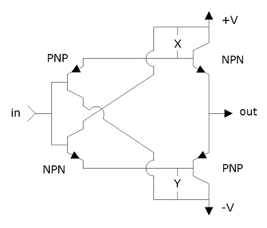
New Audio Amplifiers The Current Amplifier The current amplifier drives the speakers. It has no effect upon the signal. It is the perfect black box which allows the voltage amplifier to drive a heavy load as if it were no load at all. Figure 1. Current Amplifier
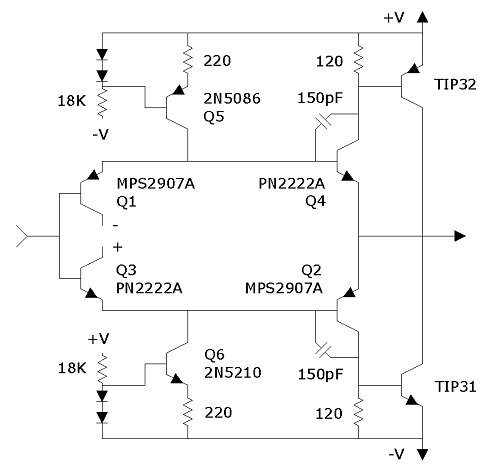
Current can be supplied to the first stage through two resistors (at X and Y), when low voltages are used, but usually current sources will replace the resistors. The current which flows through the output transistors when there is no signal is called "output quiescent current," and it is being represented by the symbol Ioq. It's value must be controlled when booster transistors are added, as with audio amplifiers. The input and output transistors must consist of two matched pairs (NPN=NPN and PNP=PNP), because they must have the same base-emitter voltages. Their betas Betas do not have to be matched between opposite type transistors, but if they are, no input current will be seen under quiescent conditions, because all of it will flow out the base of one input transistor and back into the base of the other. Figure 2. 40V Current Amplifier for Audio.
This current amplifier is functional down to about 5V and up to 40V or ±20V. It has a ripple rejection of 68 dB or better, increasing with the load. The transistors Q5 and Q6 are current sources. They supply a constant current through their collectors, in this case about 2.7mA. More current is OK, if heat is no problem. To calculate the current through the sources, there will be about 0.6V across the resistor at the emitters (220W), because there are 2 diodes from base to rail, each having 0.6V, and the base-emitter junction has about 0.6V. The current which flows through the output transistors when there is no signal is called "output quiescent current," and it is being represented by the symbol Ioq. It's value must be controlled when booster transistors are added, as with audio amplifiers. It is measured as the voltage across either of the 120W resistors. The Ioq of this current amplifier must be atleast 1 mA. It will be approximately the same as the current through the sources (2.7mA), when the input and output transistors have the same betas. When the input and output betas are not matched, the Ioq will not be the same as the current through the sources. If the input transistors have the higher betas, the Ioq will be less than the current through the sources. For example, consider these betas: Q1=135, Q2=125, Q3=185, Q4=165. The inputs are both higher than the outputs, so the Ioq will be less than 2.7mA - maybe 2.0mA. Q3 and Q4 should be reversed, which would increase the Ioq to something like 3.0mA. If in doubt, the entire current amplifier can easily be set up on a breadboard for testing. Boosters can be omitted, but they should be safe if located close to the output transistors. The size of the 120W resistors must be tailored to the Ioq, so the boosters are off during quiescent conditions. That means about 0.3-0.4V across those resistors. When the booster transistors heat up, their base-emitter voltage decreases; so there must be a wide margin in closing them. The booster transistors are attached to aluminum for cooling. Wires going to them cause them to ring at 20-40MHz. Since ringing depends upon energy being stored in wires due to their inductance, it cannot occur at low frequency. Using short wires between boosters and the rest of the circuitry reduces the tendency to ring, but a complete absence of wiring is not totally feasible, and therefore capacitors (150pF) are used to limit the speed. Those capacitors produce a very linear slew rate for the current amplifier, because they are acted upon by current sources. To determine the slew rate, the formula is V/S = I/C. It reads: volts per second equals current over capacitance. Slew rate is expressed as volts per microsecond; so the result is divided by 106. The current in the calculation is that produced by the sources. For example, in the above circuit, the current is 2.7mA, and the capacitor is 150pF. So the slew rate is (I/C) 2.7x10⁻³/150x10-12/106 = 18V/µS. If need be, the slew rate could be set as low as 5V/µS and still be fast enough for audio purposes. If wires to the boosters are 5 inches (12.5cm) long or more, only trial and error can determine the requirements for controlling the ringing. Bunching of wires to the boosters increases ringing, and therefore, headers should not be used. The recommended procedure is to put the entire current amplifier on the same aluminum plate as the boosters, as shown later. Besides making ringing easy to control, it eliminates a clutter of wires. Long power supply wires also contribute to ringing; but they only become significant when long wires go to the boosters. Because of such complexities, precarious circuits should only be tried when a scope is being used. The ringing must be thoroughly controlled, because it will cause the boosters to lock open and burn out. Under precarious conditions, the ringing might appear to be controlled when testing with a resistive load; and then speakers with long wires will cause ringing to break out. But with the conservative designs shown, the ringing is easy to control.
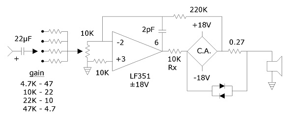
Figure 3. shows the simplest form of the audio amplifier. It uses a single op amp and a moderately high impedance (220K) feedback resistor, so input current is low. The input current is calculated as the maximum output voltage divided by the feedback resistor. The feedback resistor could be reduced to 47K and still only draw 0.35mA of input current, which should be acceptable. Figure 3. Basic Audio Amplifier
The current amplifier can be included in the feedback loop as shown, which removes offset voltage at the output. Or feedback can go from the op amp output back to the input. There would be a few tenths of a volt across Rx creating output offset, but that amount should be no problem; so the feedback resistor can be connected to the output of the op amp (removing the C.A. from the feedback loop), which increases stability, if circuits are precarious, like a lot of wiring to the boosters. The volume control is used on the inverting input, which minimizes gain and simplifies. A noninverting volume control could be used. With the inverting volume control shown, the potentiometer should be about twice the size of the smallest input resistor, and never more than five times as large. The reason is because it produces its own logarithmic taper in proportion to the input resistor. Everything above the wiper is added to the input resistance in determining the gain. So if the potentiometer is five times large than the input resistor, the gain is reduced to half, when the volume control is only 20% down. The gain formula for the inverting amplifier is the feedback resistor divided by the input resistor. The gain on the offset voltage is the feedback resistor divided by the size of the volume control potentiometer. It is low enough that no trimming of offset voltage is necessary. The feedback capacitor compensates for input capacitance and stray capacitance which produce overshoot. Overshoot shows up as a spike on the leading edge of a square wave. It does not show up on a sine wave; but removing it seems like the prudent thing to do, particularly if the amplifier is going to be used for laboratory purposes. If a scope is not being used, the following formula indicates the approximate amount of feedback capacitance required to compensate for input capacitance. If there is stray capacitance on the board, an additional picofarad or two might be needed to compensate for it.
If your browser doesn't read this, it says "picofarads (feedback) equals 1000 divided by the square root of the feedback resistor." Stray capacitance is caused by the proximity of other voltages, including ground, to the high impedance area of the inverting input. The high impedance area is that part of the wiring which is isolated by large resistors. The mass of wire on the inverting input also contributes to stray capacitance. Stray capacitance should be minimized by keeping at least 2mm of space around the inverting input, and even more around wires connected to it, and by minimizing the length of wire connected to it. When the volume control connects to the input, the op amp is located near the potentiometer, and a stiff wire goes to it for straight line routing. The noninverting input is not affected by stray capacitance. Sometimes a resistor is connected to it for protection, as shown; but it should not be necessary with FET inputs. The feedback capacitor reduces the bandwidth in proportion to its size and the impedance. The following table shows the largest feedback capacitor that can be used with a particular feedback resistor, while maintaining a flat bandwidth up to 20KHz.
Above 220k, the bandwidth depends upon stray capacitance. With a clean board, a 1 meg resistor will allow a 20kHz bandwidth. When the C.A. slew rate is reduced to 5V/µS, the overshoot spike is increased; and then the feedback capacitor is increased by 50% or more. Current through the sources should also be increased when increased stability is needed. In determining the number of gain positions to use, here are some general concepts. The lowest gain is most convenient around 3 to 5. The highest gain should be able to produce full output voltage from signals as low as ±0.2V. A typical signal is ±0.5V. Since a bridge amplifier produces four times as much wattage from any voltage, its gain should start lower; but the size of increments should be the same as for other amplifiers. The smallest step desirable for each gain increment is a factor of 2, the largest, a factor of 4. When a rotary switch is used, I would suggest a factor of 3, which reduces switching compared to a factor of 2. With the 10W amplifier, a toggle for gain select is highly convenient. The low gain is then set at about 10 or 15, and high gain at about 50. That much jump between gains is not ideal; but the convenience of a toggle justifies it. With high gain and low impedance circuitry, the input resistor gets small; and additional resistance on the line must be taken into account. For example, I put a 1k resistor on each line as it comes in to protect sources from shorting in the mono mode. The 1k resistor becomes significant when the input resistor is small. If the input resistor is supposed to be 4.7k, substitute 3.9k; and the total with line resistance will be 4.9k.
|
|
||||||||||||||||||||||||||||||||||||||