 |
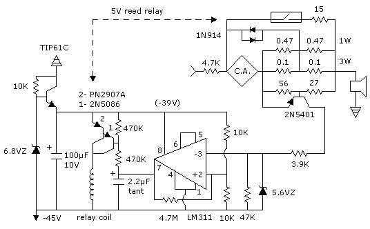
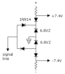
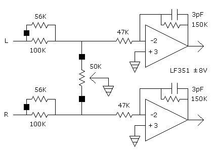
New Audio Amplifiers Output Protection Output protection by current limiting is more convenient than usual, consisting of two diodes from the protection resistor going back to the input of the current amplifier. The diodes are fast and stable. The voltage across the protection resistor at cut-in is a little less than 0.6V, because there is a slight increase in the base-emitter voltage of the output transistors when loads are heavy. For example, the 10W amplifier has about 0.57V max across the protection resistor, while the other two amplifiers have about 0.50V. The current limiting must be set for peak voltage, not rms voltage. (Rms is 0.707 times peak voltage.) The resistor at the output of the op amp (Rx) is used to prevent the op amp's protection circuit from cutting on and off creating an oscillation, when the protection diodes are conducting. With current limiting at the output, low power amplifiers are virtually indestructible. But with high power amplifiers, current limiting creates so much over-wattage on the boosters during short-out to ground that it might do no more than create a false sense of security. When short-out to ground occurs, all of the heat that would be on the speakers and about 50% more gets dumped onto the transistors. Therefore, I put over-wattage protection on the 90V amp, but not on the 10W or bridge amps. Wattage is viewed as the equivalent of heat in electronics. The heat is located where resistance or impedance creates voltage from current flows through it. Below is an over-wattage protection mechanism which removes heat from the circuits by cutting the signal for a timed interval when the current exceeds a certain level. (Figure 4.) Figure 4. Over-wattage Protection.
A capacitor delay holds the signal off for about 1.5 seconds. Diode current limiting must be used with it, because there is about a millisecond of delay in the response of the relay. The diode mechanism is set here at 6 amps (for the 90V amplifier); and the other mechanism at 5 amps. The latter must be set lower than the first, or it won't cut in. A reed relay is used to cut the signal because of its absence of voltage and two directional conduction. A 15W resistor is used on the relay line, because it improves stability by allowing about 0.5A to be conducted to the load. A few milliamps of current flow through that resistor from the output of the voltage amplifier. Since there can be variability in resistors and junction voltages, for exactness, the cut-in currents should be tested. To use a different output current, change the fractional resistors only and keep them both the same. Above, they are 0.082W. If they are changed to 0.1W, the diode protection should cut in around 5A, and the relay around 4.2A. Low impedance amplifiers are preferred, because they are slightly more resistant to noise pick up, considerably more resistant to radio frequency interference (RFI), less sensitive to stray capacitance and much faster making designing easier. The feedback capacitor can be quite a bit oversized with low impedance. Figure 5. Low Impedance Audio Amplifier
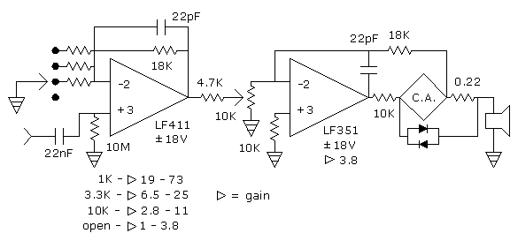
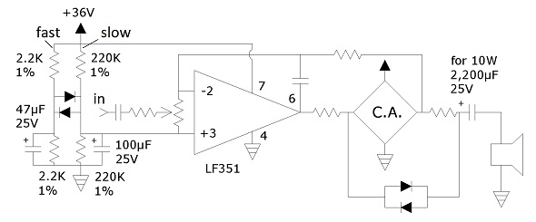
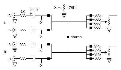
The gain for the main amp should be set at about 3 or 4 to minimize the probability of clipping by the preamp. In other words, the preamp only needs 1/3 or 1/4 of full volume that way. The preamp should not be what is called a preamp, because they are designed for picking up very weak voltages; and they, are not easy to use for this purpose. Op amps are used for all signal handling, because they are designed for that purpose. The feedback resistor for the main amp is 18K; so it creates a load of 1mA at full volume for the preamp. The preamp is an LF411 because of its low offset, which eliminates the need for a coupling capacitor between the two op amps. The input coupling capacitor (0.022µF) is tailored for the 10M resistor, as described later for coupling capacitors. The gain select resistors are switched to ground; and the gain formula changes to that of a noninverting amplifier, which is this: Gain = R-in + R-feedback / R-in. If split power supplies are not possible because of battery powered devices, the same circuitry can be used; but centering and output capacitors must be added. These capacitors reference the signal to a voltage halfway between the ground and the positive voltage. The centering capacitor creates the equivalent of a false ground for the volume control and the noninverting input. The circuit below shows how to create a very high ripple rejection by using two centering capacitors creating a slow line and a fast line which are linked together through diodes. The fast line takes the voltage to within 0.6V of center (at turn on); and then the diodes cut it off. The voltage for the centering lines should be the same as that of the op amp, so the op amp is always operating half way between its two voltages. (Figure 6.) The slow line shown here has a ripple rejection of 80dB, which is quite a bit. If the supplies are quiet or regulated, one line between the extremes should suffice. Figure 6. Nonsplit Power Supplies
The size of the output capacitor is determined by the amount of current involved and its ripple current rating. Using an oversized one allows lower frequencies to be conducted. Coupling capacitors serve as automatic voltage level shifters. Each side seeks the average voltage that it sees. The rate at which it moves to that voltage at start up depends upon the line resistance impeding the flow of current. However, it is not exactly the average voltage that is centered; it is the voltage integrated with time. This quantity is about the equivalent of average power. This technicality shows up when the signal is a square wave with something other than a fifty percent duty cycle. The peak voltage will not be the same distance from the reference voltage on both sides of the wave, because the area under the wave curve must be the same for both halves of the wave. Here is what one sees:
The coupling capacitors must have the right relationship to the impedance. If they are oversized, they take too long to center when they start up from an off voltage. With these amplifiers, the voltages are usually near ground level at start up; so the capacitors can be oversized without much slide in voltage. The minimum size for the capacitors is dependent upon the lowest frequency and impedance. An undersized capacitor will not conduct low frequencies at full volume, because the voltage slides toward center during each half of the cycle. For audio frequencies, a suitable combination of coupling capacitors and line resistors is this:
The resistors are those on the signal line such as the ones which set the gain. When a coupling capacitor connects to very high impedance, such as the input of a FET or closed switch, a resistor to ground references the voltage on the high impedance side of the capacitor. These capacitors are a little larger than is sometimes used, which allows them to produce a flat response down to 5Hz. When switching gain positions, more than one coupling capacitor might be used. I often switch one coupling capacitor for two gain positions, except with the ultra simple design, where one capacitor for four positions is adequate, because it can be considerably oversized with no problems.
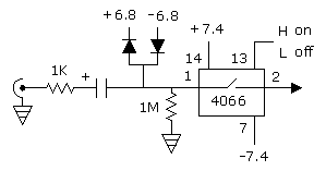
With electronic switching, the input capacitors are moved ahead of all of the switches, so the voltage is centered at ground level before going through the switches. Four capacitors are then used. CMOS switches (4066) have a maximum voltage of 15V. It is used as ±7.5V. The incoming signal should not exceed the supply voltage; so protection diodes are used infront of the first switches on the lines. The protection diodes take off at 0.6V inside the supply voltages (±6.8V), so the signals max at the supplies. If zeners are used for the supplies, they have diodes with them to set the 0.6V.
Zener diodes have quite a bit of variation; so they should be pretested at the current levels used, or the next size lower should be used. Small regulators could be used. The incoming signal would be switched in this manner:
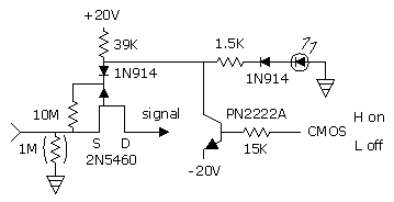
The 1M resistor to ground defines the voltage on the capacitor when it is isolated by the switch, so turning on the switch does not throw an offset voltage on the line. Its size can be optimized by making it ten times larger than the largest resistor on that line. It then produces no more than a 10% alteration of the capacitor's effectiveness. Making it much larger would allow it to create an offset voltage of its own, because the leakage current through the caps can be significant. The CMOS switch produces no significant current or voltage when off. FET switches work fine; but they are a little harder to construct than CMOS switches. Their only advantage is that they handle more voltage; and that is only relevant when tone controls are used. Even then, CMOS switching can be used with tone controls, when they are tailored appropriately, as was done with the 90V amplifier. The most commonly available 40V FET is the 2N5460 PFET, which was tested for switching on a 10W amplifier. Its design is this: (Fig)
The on resistance of this FET is about 500W or more, which must be taken into account for high gains. There are 40V NFET choppers which have a very low on resistance, such as the PN4393 or PN4092. The pinch off voltage should not be high, because it is wasted voltage. If an NFET circuit is used, it would require opposite voltages. The 10M resistor is what opens the FET when it is conducting. The shutoff mechanism requires the 1M resistor to ground whenever the incoming side might be isolated, such as a disconected input line or a coupling capacitor might cause. Here, it is used only on the four lines coming in. Otherwise, the signal defines the source voltage allowing shutoff to occur. An improper shutoff puts a biase voltage on the line. Even a complete shutoff will put a biase voltage on the line when exposed to it as occurs when switching the gain setting resistors. Therefore, a coupling capacitor must be located after the gain setting resistors and just before the volume control. The incoming capacitors might be eliminated, because the FETs handle a lot of voltage. Digital CMOS circuits open and close the FET switche through a bipolar transistor. The negative voltage for the CMOS must be the same as the emitter voltage, which in this case is about -20V. A zener diode then sets the positive voltage for the CMOS at 5V higher. The LED indicator should have a diode with it in series, because LEDs are not specified for 20V reverse which can cause them to conduct. When these circuits are switching 4066 CMOS, they should use the same voltage as it. To Digital Switching Figures
Flip flops function as two position counters for the line select and stereo-mono. A 4017 counter is used for gain select. It recycles from the high position to the low position, when the 15 pin is connected to the count above the highest used. So to get to the low gain, one must go through the high gain. There is no difficulty in doing this with medium powered amplifiers; but for high powered amplifiers, an up-down counter is better. Separate swithces are then used for up and down. Such a circuit is shown later for the 90V amplifier. Using more than two lines coming in for each channel might often be desireable; and then the line selector would have to be a 4017 set up like the gain select. Digital counters must be operated with bounceless switches, or switch bounce would often cause them to move more than one position. The bounceless switch shown can be used at any CMOS voltage without much change in characteristics. The output of the schmidt trigger goes into the clock pin of the counters.The LEDs can be controlled with 74C901 inverting buffers. These buffers sink more current than they source; so they are operated on the negative side. Their inputs tolerate overvoltage; so the plus supply only has to go up to ground level. Infact, it is two diodes below ground; so the reverse voltage on the LEDs does not go over specifications. In the 10W amplifier which used digital switching, all of the switching circuits were put on a lower board; and only the op amps and current amplifiers were put on the upper board.
A lot of features were added to the 90V amplifier in order to evaluate them. Eight gain positions were used with up-down counters and a clock for the motion. Besides two push buttons for the gain of each channel, there are two more for controlling both channels simultaneously. The latter could be omitted. Two bargraphs were used to indicate the gain position of each side. The unused LEDs on the bargraphs were concealed behind the panel. If the amplifier were used for stereo purposes only, one set of switches and one bargraph would probably be adequate. Construction would be a little easier if the bargraph were replaced by eight small LEDs. Infact, the number of gain positions could be reduced to five. The bargraph had a high visibility; so a lens was not required. Pretesting the bargraph for visibility is advised. If contrast needs to be enhanced, windshield tinting might be used rather than a lense. If rotary switches are used, six gain positions would probably be more desirable than eight for the 90V amplifier. A gain limiter was put on the front panel. It consists of a rotary switch which stops the counter at a selected upper limit. The Balance Control
The black boxes are electronic switches such as 4066 CMOS. The balance control has ideal characteristics. First, it is nondistorting, as it functions as a resistor divider on the signal line; and then an op amp returns the signal to unity gain. The center half of the potentiometer motion produces a linear response, as one side decreases at the same rate the other increases. Then towards each edge, the boosting discontinues, while the cut drops to zero. The total boost is about 1.25. To create these characteristics, the resistor divider should have a ratio of 1 or 2 to 1 at center position. This ratio is the incoming resistance divided by the resistance on the potentiometer, or one half its size. The op amp then has resistors which set its gain equal to the reduction, or about 3. In order to maintain unity gain in both the on and off position, a parallel resistor is switched also. If the balance control is not switched, only one resistor is needed 39K. (Controls)
The tone controls were tailored to do more cutting than boosting, so the resulting signal would not have too much voltage for the CMOS switching. The user does not see that fact, since the flat response centers half way between cut and boost. However, the net gain is about 1/2 at center position. This result is only detectable as a change in volume when the tone controls are switched. If it mattered, an op amp with a gain of 2 could restore unity gain; but it was not done here. The treble centers around 1kHz. It boosts to 1.8 and cuts to 0.13. The bass produces a strong effect at 300Hz and lower. It boosts to 2.0 and cuts to 0.12. The center position is flat and gains at 0.5. A bypass switch should always be included with tone controls, so distortionless sound is available without having to watch the position of the tone controls. A mechanical switch was used for the bypass, since that switch is not often used. A header was used for that switch; and it does not produce too much channel crossover, though the wires have thick insulation to minimize the problem by keeping wires separated a little. Separate op amps were used for the tone controls, so spacial arrangements could be controlled easily. The entire tone control circuitry was located on the edge of the board; and stiff wires went up to the potentiometers. A header might have been used without too much pickup or stray capacitance. Dual potentiometers were used for tone controls; so both channels could be controlled simultaneously. The edge of the board looked like this: Fig.
|
|
||||||||||||||||||||||||||