 |
New Audio Amplifiers The Quad Input Amplifier High voltage amplifiers are not commonly available on ICs. In the past, constructing them from discretes was a little cumbersome. But this new voltage amplifier, made possible by the current amplifier, reduces the problem to simplicity.
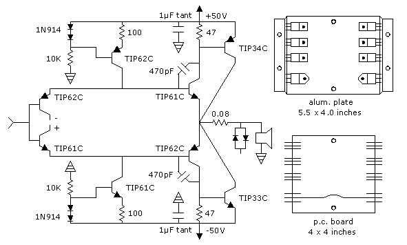
An important characteristic of this amplifier is that temperature drift is minimal, because it occurs by about the same amount in both directions. For this reason, FET inputs are feasable, even with their high drift. However, FET inputs are not needed, because another important characteristic is that the input current is gained through two stages rather than the usual one. If the betas are similar for the transistors, the quiescent input current dissapears by going through both bases. (Fig) Quad Input Amplifier Circuit
The internal gain (analogous to open loop gain) can be quite high for this amplifier. However, it reduces rapidly with a load; and even the feedback resistor will bring it down to 10,000 or less. If FETs are used on the input, the internal gain will be a maximum of 1,500; and the feedback resistor will reduce it to about 1,000. That is still sufficient gain for audio purposes. Infact a gain of 500 is sufficient. However, in these circuits the feedback resistor does not load the output, because it connects to the current amplifier. Another important characteristic of this amplifier is that it has a very high slew rate, which is needed when high voltages are used. I have measured the slew rate as high as 115V/µS. That's five times faster than the fastest commercially available op amp of this sort. A small feedback resistor, 22K, and a gain of 5 are required for that slew rate. Under the conditions used here, the slew rate peaks at 40V/µS. However, unlike most amplifiers which have a fixed slew rate, the slew rate here increases as the output supply voltage increases. The net result is that the maximum possible frequency will be about the same at any output supply voltage. The voltages supplying current to the first stage must be stable. Variations in the current will influence the Ioq. If one side only is varied, the offset voltage changes. So a trimmer is used to adjust the offset in that manner. But since the Ioq also varies, minimal trimming should be done. To minimize the trimming, the zeners should be pretested for similarity within atleast 2%. Otherwise, voltage regulators should be used. If the zeners are too low in voltage, there won't be enough output quiescent current, and an output offset will be negative. Then the 4.22k resistor needs to be smaller. If the circuit is not pretested on a breadboard, then an additional trimmer on the negative side could be used, and 2k might be preferable for the trimmers. The input transistors do not have to have a high voltage rating, provided that some of the voltage on the right side is taken up with resistors. Here, the voltage rating is high enough; but resistors (27k) are added to take some of the heat off the transistors minimizing drift. The current through those resistors is 1/2 the current supplied to both sides of the input stage, which is 0.55mA through the resistors. If the power supply has a lower voltage rating, the 27K resistors should be smaller or removed. Since the power supply voltage drops with a load, the resistors cannot be marginal in size. The output of the quad input amplifier might use TIP61C & 62C for handling more heat. The quiescent current could then be increased. The only reason for using such a low quiescent current was to minimize the heat. The thermal noise of the quad input amplifier is about twice that of a one sided amplifier, which amounts to about 3mV. The 475W resistors between the emitters of the inputs hold down the thermal noise. The output noise is not gained; and at 3mV, thermal noise is not audible on speakers. You won't find a higher quality voltage amplifier in terms of stability, speed and absence of resonance. There are three reasons: One, there are only two gain stages instead of the usual three. Two, there are no internal capacitors. And three, the emitters are close to the rails.
Power transistors are used throughout the high voltage current amplifier to dissipate heat. The input and output transistors should be attached to the same aluminum to equalize temperatures and minimize drift in Ioq. The current sources do not have to be attached to aluminum. The rail capacitors can be 10µF aluminum electrolytic instead of tantalum, but they take up more space on the small board. The power transistors can be attached to a plate with the boosters. With the plate shown, the p.c. board is above the plate, with wires extending over the edge for attachment to the transistors. The copper side is down. An over-wattage mechanism can be crammed onto the same board, with careful designing. The plate is attached to the back panel for cooling. The ratings for TIP33C & 34C are 10A, 100V, 80W. You can use TIP35C (NPN) and TIP36C (PNP), rated 25A, 100V, 175W. They are presently available at Mousers. The voltage across the protection resistor is 0.50V (6 amps) at cut in, depending upon the nature of the protection diodes.
The preamplifiers are op amps. They do not have to be the things called preamps. The specially designed preamps have the purpose of picking up weak signals as noiselessly as possible. These signals are not weak; and they are handled more easily with op amps. A 5pF capacitor was found to be suitable for the feedback of the preamps used here. Feedback capacitors can usually vary by as much as 50% without producing much distortion. The highest gain shown on this chart could be omitted, particularly if tone controls are not reducing the gain. A gain of 180 will reach down to ±0.2V signals while producing a maximum output voltage, which is quite adequate. A typical signal is ±0.5V or more.
The black boxes are 4066 CMOS switches. Each line coming in has capacitor coupling on it, so the signal is centered before going through the CMOS switches. Where a switch is on, the ground referencing is provided by a feedback resistor which holds the inverting input of the op amp near ground level. Where a switch is closed, ground referencing is provided by a 470K resistor. The resistor sizes vary for the gain setting circuitry, as indicated in the righthand column of the gain chart. Protection diodes for the switches are placed infront of the four switches at the input only. Elsewhere, signal voltage is limited by the supply voltages for the op amps. Two separate diodes must be used on each signal line. At the balance control, all four CMOS switches are switched simultaneously using the same signal. A couple of wires with heavy insulation go from the CMOS switches to the potentiometer for the balance control. At the same time the balance control is being switched on, the volume control for the left channel moves from the left control to the right control. A mechanical switch is used to minimize stray capacitance. It must be a 3PDT. Two of the poles are used to isolate both sides of each potentiometer. The third pole is used to,control the CMOS. The right channel volume control does not have to be switched. Digital Circuits for 90V Amplifier Most persons won't have time to add digital switching. Instead rotary switches can be used for variable gain. A 6P2T rotary allows 6 gain positions, which is adequate. Digital circuits are on page 5. If you want to skip over it, you can proceed to page 6.
|
|
||||||||||||||||||||||||||||||||||||||||||||||||||||||||||||||||||||||||